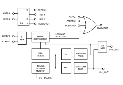
Clock&Timing - Application Specific: A Dedicated Chip That Helps Produce Signals on the Circuit Board
Static timing analyses include register-to-register analysis, I/O analysis, and asynchronous reset analysis. To verify circuit performance and detect timing violations, the Timing Analyzer uses data required times, data arrival times, and clock arrival times. In order to verify circuit performance and detect possible timing violations, the Timing Analyzer uses data arrival times, data required times, and clock arrival times. For the design to function correctly, the Timing Analyzer determines timing relationships and compares arrival times against required times.
Static timing analyses include register-to-register analysis, I/O analysis, and asynchronous reset analysis. To verify circuit performance and detect timing violations, the Timing Analyzer uses data required times, data arrival times, and clock arrival times. In order to verify circuit performance and detect possible timing violations, the Timing Analyzer uses data arrival times, data required times, and clock arrival times. For the design to function correctly, the Timing Analyzer determines timing relationships and compares arrival times against required times.

ClockTiming - Application Specific.png
Clock Setup Check
In order to determine the setup relationship for each register-to-register path, the Timing Analyzer analyzes each launch and latch edge. The Timing Analyzer uses the launch edge closest to the latch edge at the destination register for each latch edge. Figure 1 illustrates two setup relationships, Setup A and Setup B. For the latch edge at 10 ns, the closest clock that acts as a launch edge is at 3 ns and is labeled Setup A. For the latch edge at 20 ns, the closest clock that acts as a launch edge is at 19 ns and is called Setup B.
In order to determine the setup relationship for each register-to-register path, the Timing Analyzer analyzes each launch and latch edge.
Timing Analyzer reports slack values based on clock setup checks. Timing requirements are met or not met with Slack. Slack that is positive indicates that a requirement has been met, while slack that is negative indicates that it has not been met. The Timing Analyzer calculates clock setup slack for internal register-to-register paths in Equation 1.
Clock Hold Check
Each possible setup relationship for all source and destination register pairs is determined by the Timing Analyzer analyzer to determine a clock hold relationship. Timing Analyzer determines hold relationships by comparing all adjacent clock edges. Each setup relationship is subjected to two hold checks by the Timing Analyzer analyzer. During the first hold check, it is determined whether the previous latch edge did not capture the data launched by the current launch edge. It determines that the data launched by the next launch edge is not captured by the current latch edge by the second hold check.

All adjacent clock edges from all setup relationships are checked by the Timing Analyzer to identify hold relationships. Each setup relationship is analysed by Timing Analyzer twice. During the first hold check, it is determined whether the previous latch edge did not capture the data launched by the current launch edge. It determines that the data launched by the next launch edge is not captured by the current latch edge by the second hold check.
Timing Analyzer selects the most restrictive holding relationship from the possible holding relationships. The hold relationship with the smallest difference between latch and launch edges (that is, latch–launch, not latch–launch absolute value) is chosen since it determines the minimum delay allowed for register-to-register communication.
When the External Discharge arrangement is used, a logic-level (DIS) pin is connected to an external resistor (Rdis) that can be used to control the discharge of the Capacitors, such as ATAVRTS2080B.
Equation 4
Data Arrival Time - Data Required Time = Clock Hold Slack
A data required time is equal to the clock arrival time multiplied by time uncertainty plus tH
Latch Edge + Clock Network Delay to Destination Register = Clock Arrival Time
Delay from Launch Edge to Source Register + Clock Network Delay + tCO + Register to Register Delay = Data Arrival Time
Using Equation 5, the Timing Analyzer calculates the hold slack time for data paths from input ports to internal registers.
Equation 5
Data Required Time = Latch Edge + Clock Network Delay to Destination Register + μtH
Input minimum delay multiplied by input pin to register delay equals data arrival time plus launch edge and clock network delay.
Data arrival time is calculated by adding the launch edge delay, the clock network delay, the input minimum delay, and the pin delay to the source register.
Input Minimum Delay of Pin + Input Pin to Register Delay = Data Arrival Time + Launch Edge + Clock Network Delay to Source Register.
Data Required Time = Lock Edge + Network Delay to Destination Register + tH
A Timing Analyzer calculates hold slack time based on the equations in Equation 6 if the data path is an internal register.
Equation 6
Data Arrival Time - Data Requirement Time = Clock Setup Slack Time
A data arrival time is calculated by adding launch edge plus clock network delay to source register, as well as tCO plus register to pin delay.
The Data Required Time is calculated by dividing the latch edge by the clock network delay to the destination register - the output minimum delay of the pin.
Recovery and Removal
An asynchronous control signal, for example, and preset must be stable for a certain amount of time before the next active clock edge. Timing Analyzer calculates recovery slack time based on Equation 7 if asynchronous control is registered.
Equation 7
The recovery slack time can be calculated by subtracting the data required time from the data arriving time
Countdown network delay to source register + launch edge delay + tCO delay + register to register delay = arrival time for data
The data required time is equal to the latch edge plus the clock network delay to the destination register - μtSU
To calculate the recovery slack time if the asynchronous control has not been registered, the Timing Analyzer uses the equations in Equation 8.
Equation 8
Data Slack Time = Data Requirement Time - Data Arrival Time
Delay in arriving at the port to register plus maximum input delay = Data Arrival Time
Clock Network Delay + Data Required Time = Longest Latch Edge + Longest Clock Register Delay + μtSU
In order for the Timing Analyzer to perform recovery analysis on asynchronous reset signals coming from ports (device I/O), you must assign the Input Maximum Delay to the asynchronous reset pin.
In the case of asynchronous control, the Timing Analyzer calculates removal slack time based on Equation 9.
Multicycle Paths
Several clock cycles are required to latch data at the destination register on multicycle paths. Every second or third rising clock edge, for example, may require capturing data in a register.
Related News
1、Chip Packaging Lead Time Has Grown to 50 Weeks
2、Eight Internet of Things (IoT) Trends for 2022
3、Demand for Automotive Chips Will Surge 300%
4、Volkswagen CFO: Chip Supply Shortage Will Continue Until 2024
5、BMW CEO: The Car Chip Problem Will Not Be Solved Until 2023
6、Shenzhen: This Year Will Focus on Promoting SMIC and CR Micro 12-inch Project


